
2026 Forecast of China’s Advanced Packaging Capacity as a Global Share
China’s role in advanced packaging is moving from “important participant” to “strategic balancing force” in the global semiconductor supply chain. By 2026, its capacity is expected to represent a meaningful share of worldwide advanced packaging output, especially in high-volume OSAT-driven segments, even as some of the most cutting-edge AI packaging still remains concentrated elsewhere. That contrast is exactly what makes the story interesting: China is scaling fast, but the global market is not all one market. Different packaging technologies, different end markets, and different levels of localization are expanding at very different speeds.
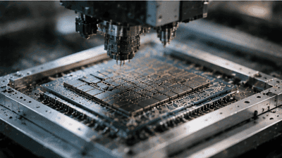
The result is a nuanced picture. On one hand, China has built a strong foundation in assembly and test, fan-out, system-in-package, and mainstream advanced packaging for consumer, mobile, automotive, and networking devices. On the other hand, the most demanding 2.5D and 3D AI packaging flows still lag in localization. So when people ask about China’s global share in 2026, the honest answer is that the country’s share is rising steadily overall, but unevenly across technologies. In some areas, China is already a major force. In others, it is still catching up.
The Big Picture
Advanced packaging has become one of the most important layers of semiconductor competition. As chip scaling slows and heterogeneous integration takes over, packaging has moved from a supporting role to a system-defining one. That means capacity in advanced packaging is no longer just about how many chips can be assembled. It is about who can deliver the most valuable, bandwidth-rich, multi-die systems.
China’s forecasted share of global advanced packaging capacity in 2026 needs to be read in that context. The country already plays a major role in mainstream packaging and high-volume OSAT services, but advanced packaging now includes a broad spectrum of technologies:
- Flip-chip and advanced wire-bond packaging.
- Fan-out wafer-level and panel-level packaging.
- 2.5D interposer-based integration.
- 3D stacking with TSVs or hybrid bonding.
- System-in-package modules for mobile, automotive, and industrial use.
China’s share is stronger in the middle of that spectrum than at the very leading edge. That is not a weakness so much as a reflection of how technology diffusion works. The question is how quickly that share can move upward as more capabilities are localized and more production lines reach maturity.
Where China Is Strong

China has already built serious scale in OSAT and packaging manufacturing. That scale matters because advanced packaging is not one technology but a production ecosystem. It requires assembly capacity, test infrastructure, materials suppliers, substrates, and increasingly specialized equipment. China has made meaningful progress in those supporting layers.
The strongest areas include:
- High-volume assembly and test. Large domestic OSATs give China a strong base in packaging throughput and customer coverage.
- Consumer and mobile packaging. Many mainstream advanced packaging formats used in mobile devices and consumer electronics are already well established domestically.
- System-in-package platforms. China has strong demand and growing capability in SiP for RF, power, sensors, and mixed-function modules.
- Fan-out and panel-level development. These technologies are increasingly relevant to high-volume consumer and industrial markets where cost and form factor matter.
This foundation supports a rising global share because these are exactly the kinds of packages that ship in large volumes. Even if they are not always the most glamorous technologies, they account for a lot of real market demand. That gives China a strong presence in the overall market share picture.
The Leading-Edge Gap
At the same time, it would be misleading to treat all advanced packaging technologies as equally localized. The biggest gap remains in the most demanding AI and HPC packaging flows. These include:
- Large 2.5D CoWoS-style packages with multiple HBM stacks.
- Advanced 3D integration based on hybrid bonding.
- Ultra-fine pitch interposer and high-density die-to-die platforms.
The reason is not only equipment. It is also process know-how, yield maturity, materials quality, and customer qualification cycles. These advanced flows need tight co-optimization of wafers, packaging, memory, substrates, and test. That takes time to build and even longer to scale into high-volume production.
China’s localization rate in these top-end segments is still much lower than in mainstream packaging, which means its global share is more limited at the very top. But that gap is also the biggest opportunity. Every step toward domestic interposer capability, hybrid bonding maturity, and HBM-related packaging increases the country’s influence in the highest-value segment of the market.
Why 2026 Matters
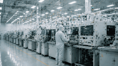
The year 2026 is important because it sits at the intersection of multiple trends. AI demand is still strong, chiplet adoption is expanding, and governments and companies alike are prioritizing supply chain resilience. That creates a favorable environment for advanced packaging investment.
For China, 2026 may be a year where several earlier investments start to show up in meaningful capacity numbers. That includes:
- New or expanded OSAT lines.
- More mature fan-out and SiP production.
- Better domestic supply of packaging materials and substrates.
- Incremental progress in high-end packaging equipment localization.
The effect is cumulative. Even if no single breakthrough makes headlines, the combination of many small gains can shift global share noticeably. In advanced packaging, capacity is not won in one leap. It is built layer by layer, line by line, qualification by qualification.
The Supply Chain Behind the Share
A forecast of global share is really a forecast of the full supply chain. Advanced packaging depends on much more than assembly labor. China’s progress will depend on the maturity of several related layers:
- Substrates and interposers. These are critical for fine routing, mechanical support, and 2.5D integration.
- Bonding and placement tools. Advanced packaging requires precise alignment, better throughput, and higher yields.
- Materials. Mold compounds, underfills, dielectrics, and thermal materials all need to meet tighter specs.
- Metrology and inspection. Yield and reliability depend on the ability to detect defects early and precisely.
- Test infrastructure. Multi-die packages need more sophisticated wafer-level, package-level, and system-level test methods.
China is making progress in all of these areas, but not uniformly. Some segments are more developed than others. That unevenness is why a global share forecast must distinguish between broad packaging capacity and high-end advanced packaging capacity. The former is already significant. The latter is still growing into its potential.
OSATs as the Engine

The domestic OSAT sector is the engine of China’s packaging rise. OSATs are where much of the volume lives, and volume is important because it builds process competence. Once a company can run high-volume packaging reliably, it has a base from which to move into more complex products.
China’s leading OSATs have been expanding into more advanced domains, including fan-out, SiP, and more sophisticated multi-chip modules. That matters for global share because advanced packaging demand increasingly comes from applications outside the AI hype cycle:
- Automotive electronics.
- Wireless connectivity and RF front ends.
- Industrial and power electronics.
- Consumer AI and mobile devices.
These are large markets with recurring demand, and they help raise China’s share even if the top-end AI packages remain constrained. In many ways, the broad base of demand is what gives China a path to larger global relevance in packaging.
What Limits Growth
The main limit is not demand. The demand side is strong enough. The constraints are more practical: tooling, process maturity, key materials, and qualification time. Advanced packaging is extremely sensitive to yield. Small deviations in flatness, contamination, alignment, or thermal stress can affect the entire package.
That is why leading-edge capacity cannot be built overnight. Domestic firms need not only equipment but also experience, process data, and customer trust. For the most advanced products, qualification cycles can be long. Customers want proven reliability before they move high-value designs into new packaging ecosystems.
In addition, some supply chain elements remain globally concentrated. When those segments are hard to localize quickly, they create a ceiling on how much advanced packaging capacity can be fully domestic by 2026. This is especially true for the most complex AI-oriented configurations.
How China’s Share May Be Interpreted
It is useful to think of China’s global share in three buckets:
- Broad advanced packaging. Here China’s share is already substantial and likely to keep rising in 2026.
- Mainstream heterogeneous integration. Here China is gaining share as SiP, fan-out, and multi-die products expand.
- Leading-edge AI packaging. Here China’s share is still relatively small, but the growth potential is the highest.
This layered view avoids oversimplifying the forecast. The market is not a single monolith. A country can have high share in one segment and low share in another. That is exactly what we see in China’s advanced packaging trajectory.
Strategic Implications
The forecast matters because advanced packaging is increasingly strategic. It determines who can build high-performance systems, who can support AI infrastructure, and who can capture value in the post-Moore’s-Law era. If China increases its share of global advanced packaging capacity in 2026, it gains leverage across the electronics value chain.
That leverage shows up in several ways:
- Greater resilience for domestic chip supply.
- More options for chip designers seeking local packaging partners.
- Improved ability to support consumer, automotive, and industrial system integration.
- Longer-term potential to move up the value chain into more demanding AI and HPC packaging.
It also has a competitive effect globally. As China’s capacity expands, other regions will likely respond with more investment, tighter partnerships, and a stronger push to secure their own packaging ecosystems. In that sense, China’s rising share is not just a national story. It is part of a broader reshaping of the semiconductor supply chain.
The Road to 2030
2026 is not the end point. It is one waypoint on a longer road. If China continues to expand advanced packaging capacity, the bigger story by 2030 may be whether it closes the gap in higher-end 2.5D and 3D integration. That will depend on how quickly domestic equipment, materials, and qualification ecosystems mature.
There is reason for cautious confidence. The domestic base is large, demand is strong, and policy support remains active. The challenge is to convert broad capacity into deep capability. That means moving from volume in established package types to mastery in the most complex heterogeneous integration flows.
If that happens, China’s global share in advanced packaging could shift from “significant” to “defining” in several key segments. If not, the country will still remain a major packaging hub, but with a sharper split between high-volume mainstream strength and leading-edge dependency.
Conclusion
The 2026 forecast of China’s advanced packaging capacity as a global share tells a story of steady expansion, uneven progress, and enormous strategic importance. China is already a major force in the packaging ecosystem, especially in OSAT-driven, high-volume, and consumer-facing segments. Its share is rising because the domestic ecosystem is getting stronger across assembly, test, fan-out, SiP, and supporting supply chains.
At the same time, the highest-end AI packaging remains more limited, which means the global share picture is not uniform. Some technologies are already close to domestic scale. Others still need time, investment, and process maturity. That mix of strength and gap is what makes the forecast so interesting.
In the broader landscape of advanced packaging and heterogeneous integration, China’s 2026 trajectory is not just about adding more capacity. It is about reshaping where the value of semiconductor integration sits, and who gets to participate in the next generation of system-level computing.
You May Like

Narrowing Spread Between NAND Spot and Contract Prices in 2026 – A Signal
By 2026, one of the most watched metrics in the NAND flash market has started to shift in a subtle but meaningful way: the spread between spot prices and long‑term contract prices is narrowing. For casual observers, this may look like just another incremental change in a notoriously volatile industry. For memory makers, module houses, device OEMs, and data center buyers, however, a tightening gap between spot and contract prices is a signal—a reflection of evolving supply–demand balance, risk perceptions, and strategic behavior on both sides of the market.

Price Divergence Trading Strategies Between NAND Flash and DRAM ETFs
NAND flash and DRAM sit at the core of AI storage and computing power. Both are memory, but they are not the same business. DRAM is main memory—fast, volatile, and central to high‑bandwidth workloads like AI training and inference. NAND is non‑volatile storage—slower than DRAM, but crucial to persistent data and large‑scale object storage. The cycles that drive their pricing and margins overlap, yet they often diverge. That divergence is where trading strategies between NAND and DRAM ETFs become interesting.

China’s HBM Localization Progress: The Catch-Up Pace of CXMT and XMC
China’s drive to localize advanced memory technologies has accelerated over the past several years. High-Bandwidth Memory (HBM) sits near the center of that strategy because it is integral to AI accelerators, high-performance computing (HPC) and other strategic compute platforms. Two domestic players—ChangXin Memory Technologies (CXMT) and XMC (Xianghui Memory, commonly referred to as XMC)—have become focal points in assessing how quickly China can close the gap with international incumbents on HBM die, stacking, and packaging.

Thermal Simulation Challenges and Solutions in 3DIC AI Chip Design
As AI workloads push chips to deliver ever higher compute density, designers are increasingly turning to three‑dimensional integration (3DIC) to stack dies vertically and pack more functionality into limited footprints. While 3DIC architectures unlock significant performance and bandwidth advantages, they also introduce complex thermal behaviors that are far harder to predict and manage than in traditional 2D layouts.

An Attempt at Compiling a Memory+Compute Fusion Thematic Index – A Dual-Track Framework
Most AI investors talk about “compute” as if it were the whole story: GPUs, accelerators, chips, cores. But every one of those cores needs somewhere to read from and write to. Memory and storage define how wide the data highway really is. In practice, AI performance is a fusion of compute and memory, not a solo act. So why do so many indices and ETFs separate them into different silos—one for semiconductors, one for memory, one for data centers—when the actual workloads keep blending them?

Surging Demand for Laser Drilling and Plasma Dicing Equipment in Advanced Packaging
Advanced packaging has become one of the semiconductor industry’s most important growth engines, and it is now pulling a surprising set of process tools into the spotlight. Among the most in-demand are laser drilling and plasma dicing equipment. These machines sit close to the heart of heterogeneous integration, fan-out packaging, wafer thinning, TSV formation, glass substrate processing, and other advanced flows where precision, yield, and throughput matter enormously. As packaging moves from a back-end afterthought to a strategic platform, the equipment used to shape, open, and separate materials has become just as important as the dies themselves.

D2D Interface Bandwidth and Latency Comparison in Chiplet Architectures
Chiplet architecture has turned the package into a real performance battleground. Once multiple dies are placed side by side or stacked within the same advanced package, the quality of the die-to-die, or D2D, interface becomes one of the most important determinants of system behavior. Bandwidth is no longer a nice-to-have metric, and latency is no longer a small implementation detail. Together, they shape whether a chiplet system feels nearly monolithic or frustratingly fragmented.

Stock Selection Logic and Alpha Validation of ESG-Themed Semi ETFs
Semiconductor themed ETFs are no longer just about growth and cycles. A growing subset now layers environmental, social, and governance (ESG) criteria on top of traditional sector exposure. These ESG semi ETFs promise two things at once: access to one of the market’s most powerful secular themes, and alignment with sustainability and governance standards. The pitch is appealing, but it raises two hard questions. First, how exactly are these stocks being selected? Second, does the ESG overlay help, hurt, or leave alpha unchanged?